
Biscuit - The Lightweight RISCV Core
1. Introduction
Sometimes you gotta risk it for the biscuit but this Biscuit is here to minimize risk. Biscuit is designed to be a lightweight RISC-V core that supports the RISCV32I instruction set. It’s lightweight nature makes it a good choice for distributed computing where multiple biscuits can be deployed to focus on and execute specialized tasks. This also enables multiple biscuits to be stacked together for TMR or other majority voting schemes to make hardened Biscuits suitable for radiation rich environments like space. Biscuit can also be useful when it comes to replacing large complex designs inside a FPGA in which case utilization can be significantly reduced when a large piece of the design is replaced by a Biscuit. Biscuit currently comes in two flavors, a single cycle flavor and a 5 stage pipelined flavor. Source code for the project can be found on Github!
2. Single Cycle Flavor
In this variant, Biscuit executes everything in a single cycle, hence it being the single cycle flavor. Meaning all the logic associated with an instruction must complete in time for the next clock edge resulting in a low maximum operating frequency. This is because the clock period must accommodate the propagation delay of the slowest instruction. The two main benefits of a single cycle design are a more predictable execution time and a smaller foot print. A single cycle core can actually be the preferred solution for certain niche applications, especially if clock speeds are not important. Regardless the single cycle variant is easier to understand and a prerequisite for understanding any pipelined variant. Below is a block diagram showing the workings of the single cycle variant.
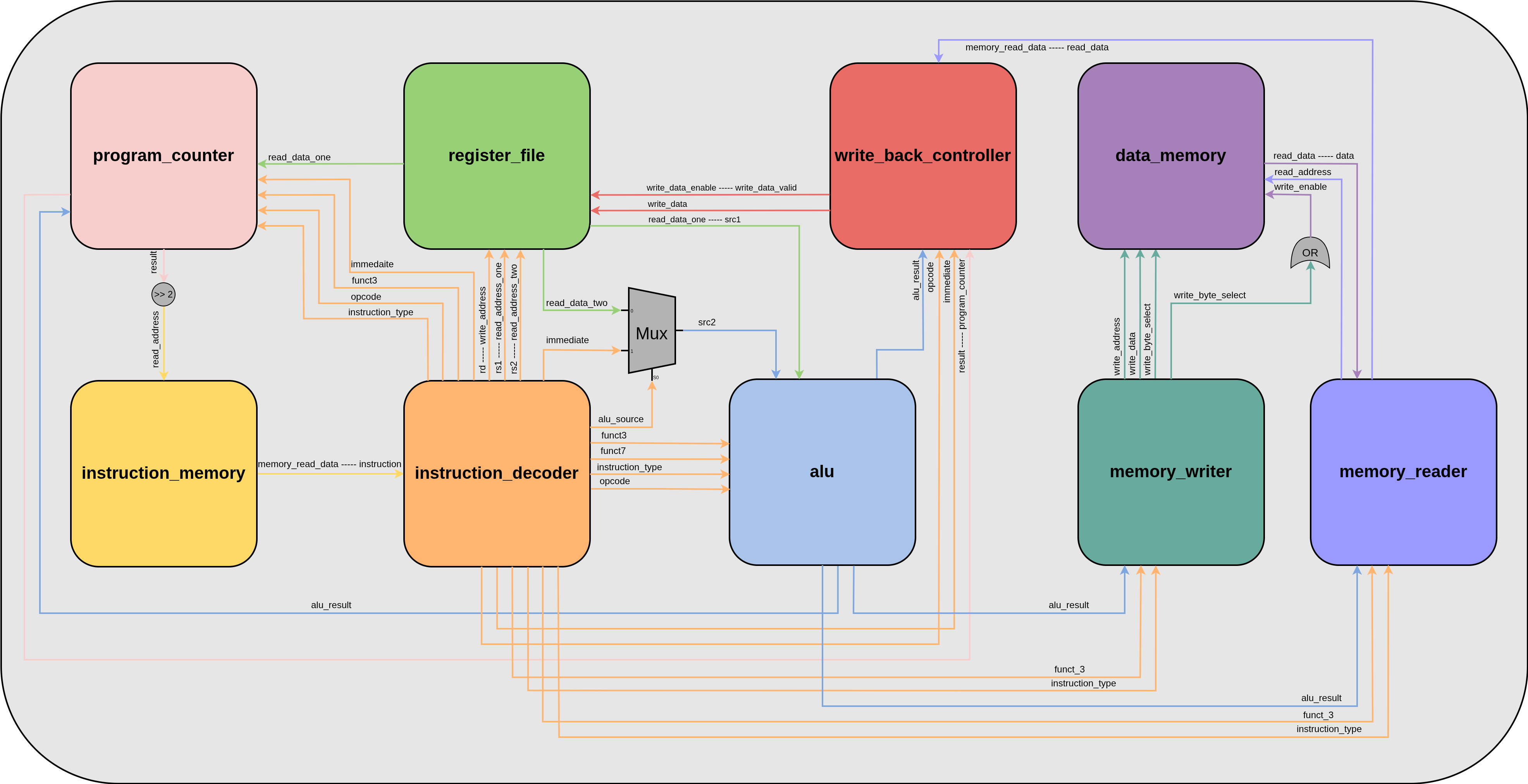
2.1 Program Counter
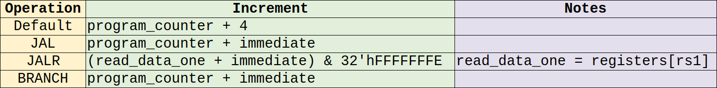
This module implements the logic needed to calculate the program counter register. “Program counter” is a 32 bit register is used as a read pointer by the instruction memory to fetch the next instruction. Each clock cycle the program counter will increment by 4. Memory addressing is done at byte boundaries and since each instruction is 32 bits, the program counter increments by 4 every clock cycle to fetch the next instruction. However some instructions like branch and jump instructions will cause the program counter to increment by a different value. Below is a table summarizing the various program counter increments.
2.2 Instruction Memory
This block contains the program instructions. Since Biscuit is currently being deployed on FPGAs the instruction memory is made up of block rams. The data width of the block ram is 32 since each instruction is 32 bits. The read address of the block ram is the program counter divided by four. To create the divide by four we shift the program counter by 2. read_address = program_counter >> 2.
2.3 Register File
This block implements the 32 general purpose registers that are part of the ISA, “x0” to “x31”. The block has one write port with “rd” as the target write address and two read ports with “rs1” and “rs2” as the respective read addresses. The module has two independent ports for “rs2”, an A and B port but this feature is only taken advantage of in the pipelined flavor. In the single cycle flavor only port A is used.
2.4 Instruction Decoder
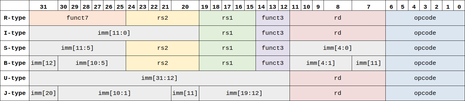
For each instruction fetched from the instruction memory, this block will parse the instruction as defined by the ISA into various control and data fields. These fields are then fanned out to relevant parts of the core. Below is a summary showing how each type of 32 bit instruction is decoded at the bit-level.
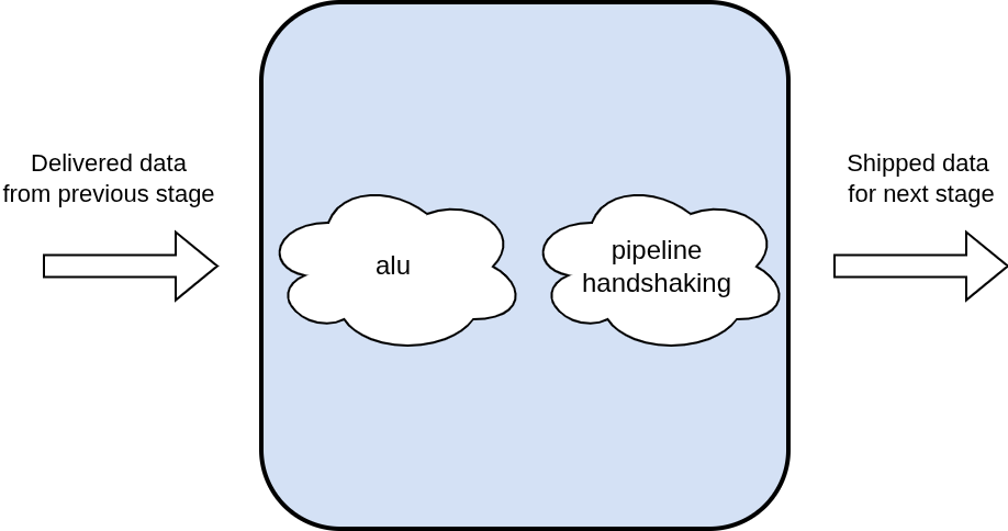
2.5 ALU
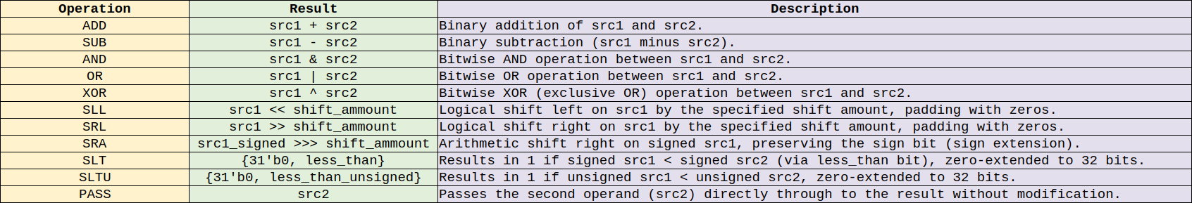
This block performs all the arithmetic operations in the core. The type of operation done and what its inputs are depend on the supplied on the supplied instruction. Below is a table showing all the support ALU operations in Biscuit and what they do.
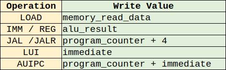
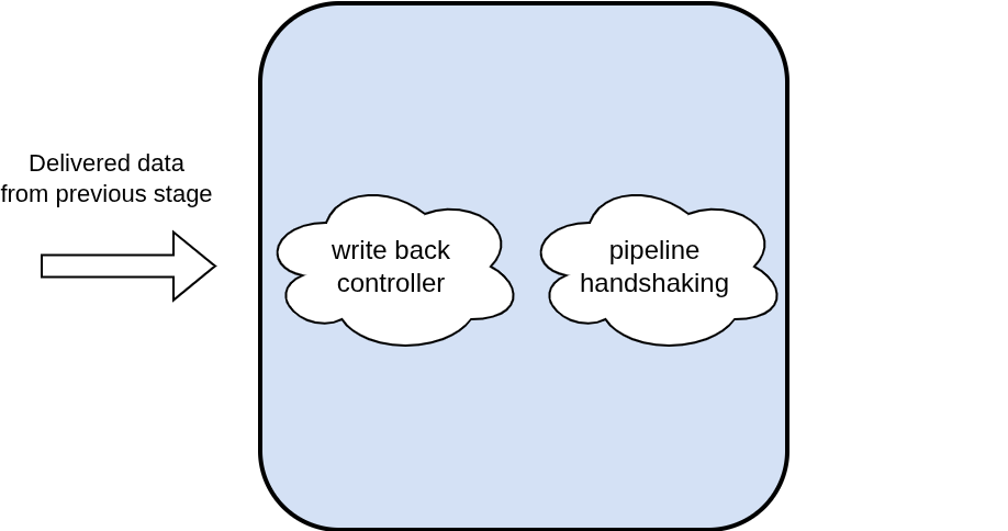
2.6 Write Back Controller
This module is responsible for calculating the values to be written to the register file with a destination of “rd” if an operation calls for it. For example if rd = 5 it will write the calculated value to x5 in the register file. Below is a table showing how Biscuit calculates the value to be written.
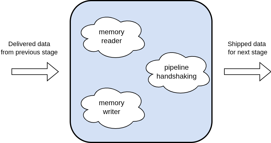
2.7 Memory Writer and Memory Reader
These two modules enable the reading and writing of memory. Their purpose is the move data in and out of memory. Data is 32 bits wide and is byte selected/masked depending on the operation. Currently data is only read and written to the data memory block ram. However, if there were any memory mapped peripherals like UARTs, I2C Masters, CAN buses, Timers, etc they could be communicated with using these modules.
2.8 Data Memory
This is the block ram that serves as the data memory of the core. The memory has a total width of 32 and is byte selectable on both read and write. To implement this there are 4 individual block rams of data width 8 that are linked together.
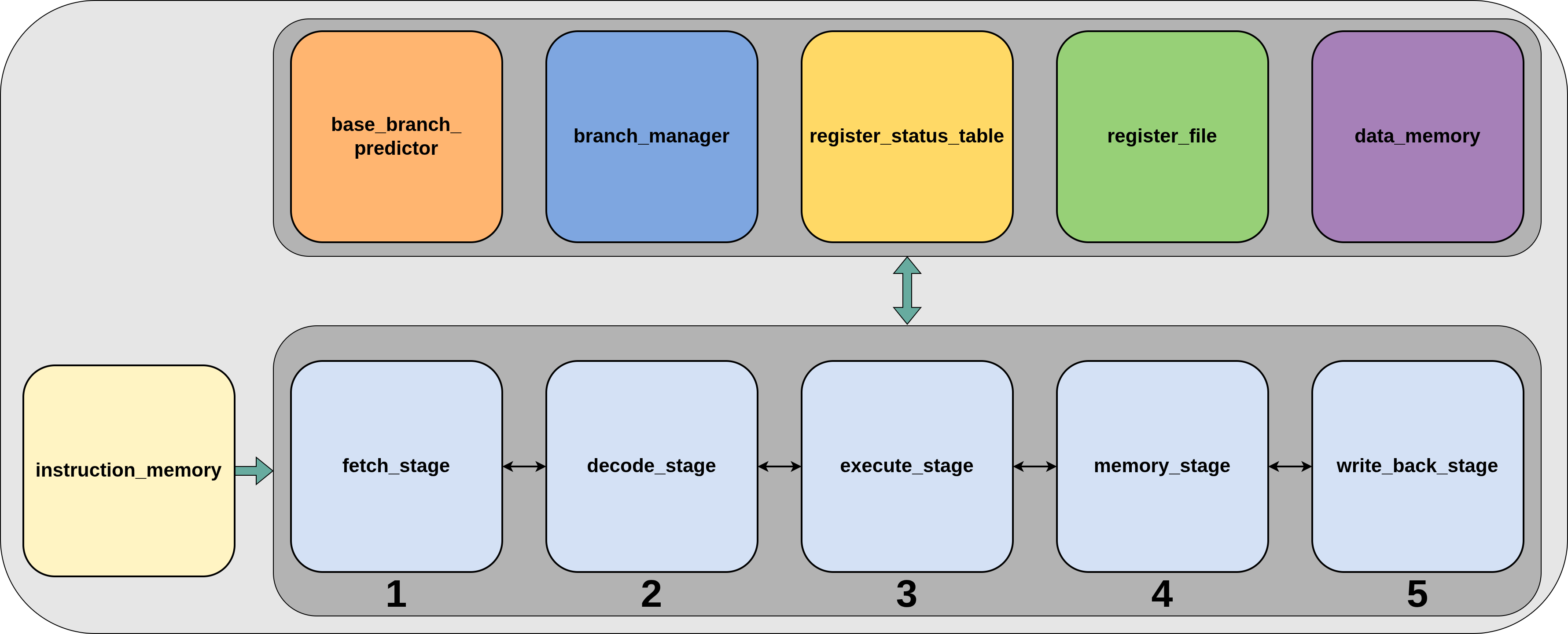
3. Pipelined Flavor
To achieve a higher operating frequency Biscuit also comes in a pipelined flavor. The pipeline chosen is the classic 5 stage pipeline. Common number of pipeline stages include 3, 5, and various deeper stages like 8. With Biscuit, 5 was chosen to strike a balance between performance and complexity. The 5 stages include in order: Fetch, Decode, Execute, Memory, and Write Back. Below is a high level block diagram showing the workings of the pipelined flavor of Biscuit.
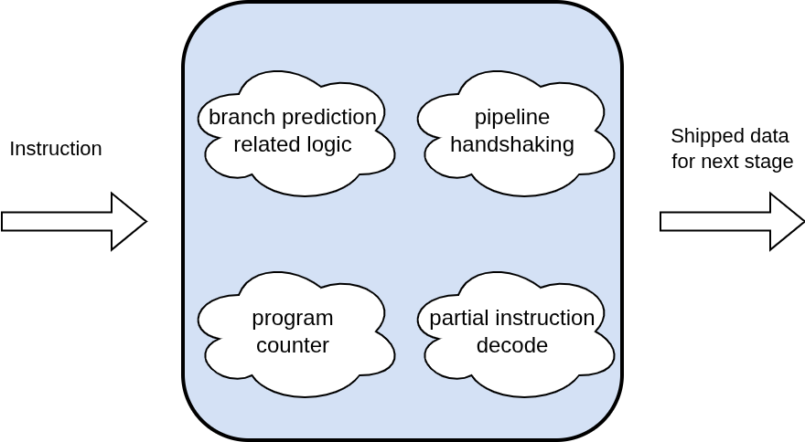
3.1 Fetch Stage
The first stage of the pipeline is the fetch stage. The main purpose of this stage is to keep track of the program counter and pull instructions from the instruction memory. It also partially decodes the instruction, just enough to calculate the next program counter value. In the event where the current instruction is a branch, the stage takes into account signals from the branch predictor. Both the branched and unbranched program counter are saved and shipped down the pipe for future processing. This is because the true branch result is calculated in the execute stage which means we will need both values to reinforce the prediction model or course correct in the event where the prediction was incorrect.
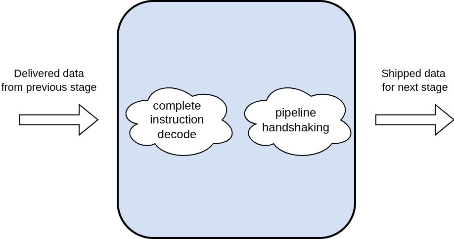
3.2 Decode Stage
The second stage of the pipeline is the decode stage. In this stage the instruction is completely decoded and the decoded values are shipped along to the next stage. In the event where the instruction is invalid, the path of the current instruction ends here. At this stage the register_status table is also updated to keep track of registers who’s values are pending since registers do not get updated until the write back stage. In the event where a register needs to be marked as busy in the status table but it is already marked busy from a previous instruction (double write hazard), the pipe is stalled at this stage until the register is not busy.
3.3 Execute Stage
This stage is responsible for doing the ALU operations. The register status table is polled to prevent read after write hazards. In the event where the execute stage detects the instruction calls for the reading of a register who’s value is still pending, the stage stalls the pipe until the read after write hazard is gone.
3.4 Memory Stage
During this stage all memory reading and writing is completed if the current instruction calls for it. Similar to the execute stage, the register status table is polled to prevent any read after write hazards.
3.5 Write Back Stage
This is the final stage of biscuit and its where the writing of registers occurs. In this stage the registers are also retired in the register status table if they were previously marked as busy.
3.6 Register File and Register Status Table
The register file used is identical to the one used in the single cycle flavor but in order to prevent hazards a register status table is added to keep tracking of which registers are busy. Because writing of registers occurs during the last stage, the write back stage, this is status table is necessary. The index of the table corresponds to the register and a value of 1 indicates that that current register is busy.
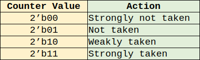
3.7 Base Branch Predictor and Branch Manager
The base branch predictor is a bimodal 2-bit predictor with a saturating counter. It is named the “base” branch predictor because this model is the base predictor of a larger TAGE predictor not included in this lightweight version of Biscuit. During the fetch stage the lower bits of the program counter are fed into the base predictor which uses it as an index into a table. If the returned counter value from the table is >= 2'b10, the branch is taken. Below is a table explaining what the counter values mean.
Once the instruction completes the execute stage, Biscuit will know if the predictor was correct or not. The branch manager monitors this and takes action based on the result. Depending on what the prediction was and what the result is, it will tell the base branch predictor to increment or decrement the counter value for the given index. When the predictor is incorrect it will also course correct the pipeline by flushing the current instruction stream and forcing it to start over with the correct branch address. The general idea is the reinforced learning mechanism will cause Biscuit to become better at predicting branches over time.
4. Implementation Results
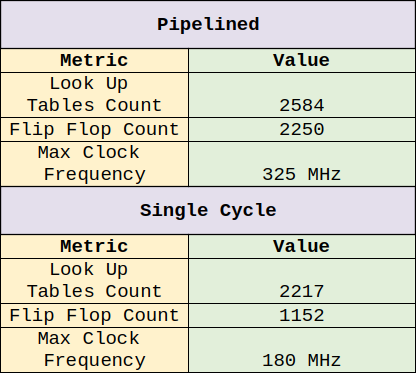
Below are the implementation results of both flavors of Biscuit on a mid range Ultrascale+ Xilinx FPGA (XCZU3EG-SFVC784-1-E). The pipelined flavor of Biscuit achieves an exceptionally good maximum clock frequency of 325 MHz with only about twice the number of flip flops as the single cycle flavor. The single cycle flavor does well at 180 MHz but of course the single cycle flavor will scale very poorly once integrated into a larger design or if any memory mapped peripherals are added to the core.
5. What’s next for Biscuit?
More heavyweight features for Biscuit may be published as they are developed for other projects. Below is a list of the top 5 features that are currently being prioritized. If you’d like to contribute and make Biscuit grow, feel free to do so on Github!
1. Floating point unit and F extension support
2. Super-scalar processing and out of order execution
3. Deeper pipelining for higher speeds
4. Interrupt support
5. 64-bit support