Discrete Gate Driver Designs
Overview and Theory
Unlike an ideal switch, the cost of switching a mosfet is the amount of charge the gate requires and the amount of power wasted as RDS swings from its max to min value. By delivering/removing as much charge as possible, in the smallest amount of time (in other words the most current) to/from the gate of the fet, we can minimize our switch time and by extension minimize our switching losses. The simplest way to model the switching requirements of a mosfet is to treat it as a capacitor. By doing so we can calculate the required power needed to switch it at a particular frequency and voltage. The energy stored in a capacitor is \(E_{stored} = 0.5CV^2\) and in the process an equal amount of \(E_{lost} = 0.5CV^2\) is dissipated. Therefore, the net amount of energy required is \(E_{net} = CV^2\). Given that \(Q = CV\) we can also use \(E_{net} = QV\). The power required to do this at a certain frequency is \(P = QfV\). With a mosfet, we are concerned about the overall gate capacitance \(C_{g}\), the overall gate charge \(Q_{g}\), and \(\Delta V_{g}\) which is the difference between the high and low of the drive voltage (for example if our gate drivers output voltage is a \( 0V\) to \(15V\) square wave, \(\Delta V_{g}= 15V – 0V \) ). Using the power we can find our minimum required current \(I_{g-min} = P/\Delta V\).
\(C_{g}\) and or \(Q_{g}\) can be found in most datasheets. However it is important to note that \(C_{g}\) and \(Q_{g}\) changes with the drive voltage. To find the accurate \(Q_{g}\), an experiment or simulation must be set up where the gate current \(I_{g}\) is measured as the mosfet is turned on. Integrating this current with respect to time will result in \(Q_{g}\). In other words, \( \int{I_{g} dt = Q_{g}}\). By knowing, the exact amount of gate charge, whether via experimentation or the datasheet, we can determine the peak drive current required for a desired switch time with the formula \(I_{g-peak} = \frac{Q_g}{desired\ switch\ time\ [s]}\).
Another thing to consider when switching mosfets is the inductance of the gate, \(L_{g}\). This includes everything from the output of your driver to the physical gate of the transistor. A typical T0-22 package mosfet can have around 7nH of gate inductance. This inductance can cause ringing and oscillation, especially at higher switching frequencies. To dampen the ringing we can place a resistor, \(R_{g}\), between the driver and gate. The resulting circuit can be modeled as a typical RLC circuit shown below.
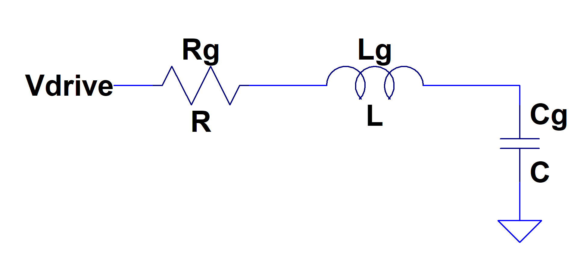
In the circuit above, the dampening factor \(\zeta\) is equal to \(\frac{R_{g}}{2}\sqrt{\frac{L_{g}}{C_{g}}}\). In order to have no oscillation the circuit must be at least critically damped with a \(\zeta >= 1\). Therefore \(R_{g}\) must be greater than or equal to \(2\sqrt{\frac{C_{g}}{L_{g}}}\). Lastly, it’s important for the gate driver to be able to drive with this new \(R_{g}\). This means the maximum gate resistance must allow the peak drive/sink current \(I_g\). Therefore, the maximum gate resistance, \(R_{g-max}\) must be equal to \(\frac{V_g}{I_{g-peak}}\).
Summary of Equations
$$Gate\ Charge:\ Q_g = \int{I_gdt}$$
$$Average\ Drive\ Output\ Power:\ P_{out} = Q_g\ f_{switching}\ \Delta V_g$$
$$Absolute\ Minimum\ Drive\ Output\ Current:\ I_{g-min} = \frac{P_{out}}{V_g}$$
$$Gate\ Resistance\ to\ Eliminate\ Ringing:\ R_{g} >=2\sqrt{\frac{L_{g}}{C_{g}}}$$
$$Peak\ Drive\ Output/Sink\ Current:\ I_{g-peak} = \frac{Q_g}{desired\ switch\ time\ [s]}$$
$$Maximum\ Gate\ Resistance:\ R_{g-max} = \frac{V_g}{I_{g-peak}}$$
Discrete Drivers
There are many gate driver ICs that can be readily purchased however it can be quick and easy to make a great drive circuit with some basic parts.
Design 1 (Low Current)
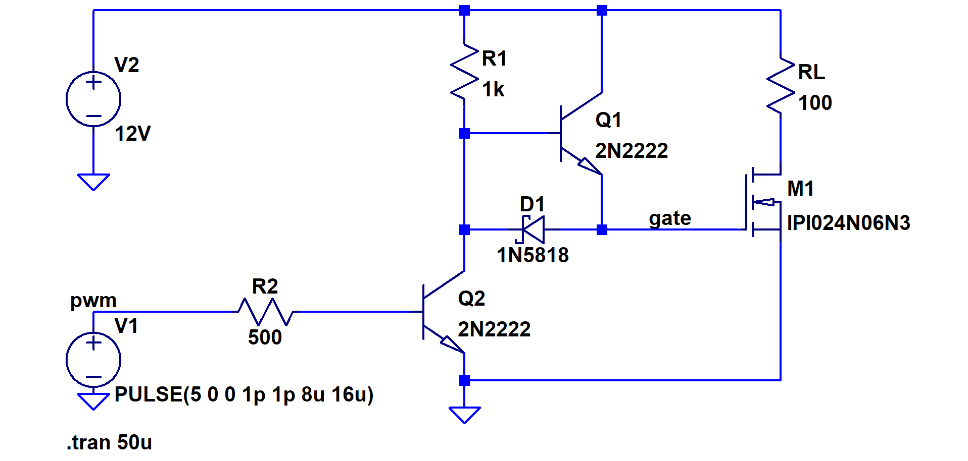
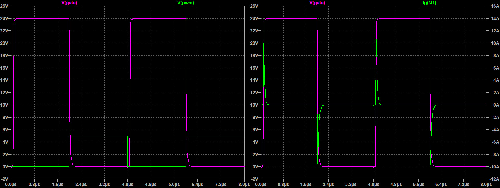
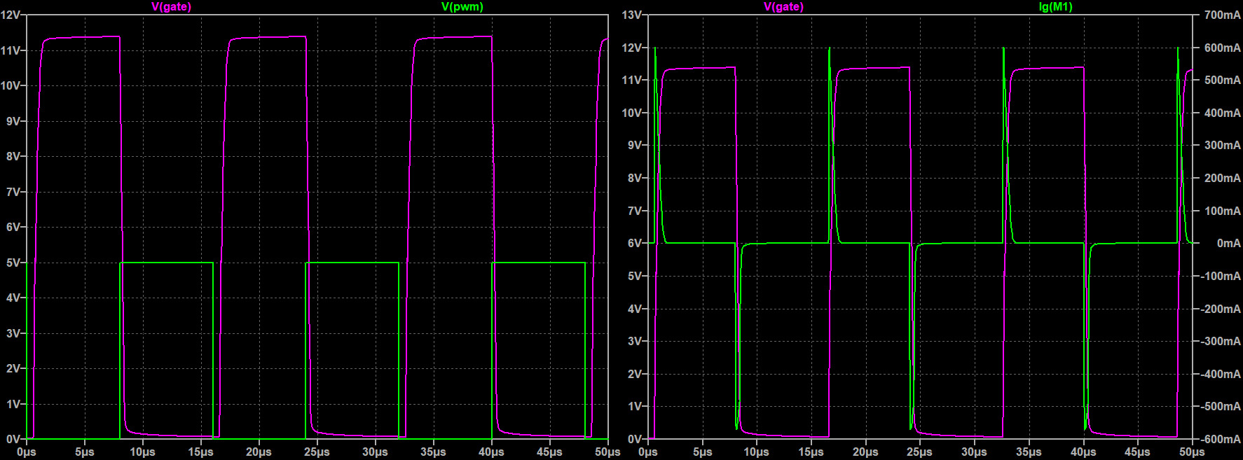
This design uses two NPN BJTs, Q2 as an inverter and Q1 to isolate the 12V voltage from the PWM control signal. When the PWM control signal is LOW, Q2 is off and Q1 is biased ON, driving Vgate HIGH. When the PWM signal is HIGH, Q2 is biased ON which brings the base voltage of Q1 to GND and creates a path to GND through D1 for current to be sinked from Vgate. The beauty of this design is in its simplicity however the output current is ultimately limited by the amount of current Q1 can deliver and Q2 can sink. With a pair of 2N222s we can achieve a maximum pulsed collector current of about 1A. As seen by the simulation results below, the above configuration nets us about 600mA of drive/sink current with a 12V rail. This design is able to sink about the same amount of current given that the sink current path is identical to the drive path except for the diode. More current can be achieved by biasing Q1 harder via a lower R1 or higher rail voltage.
Design 2 (Medium to High Current)
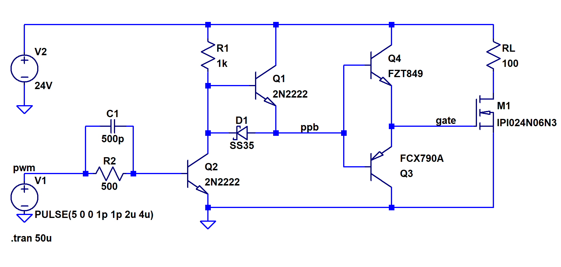
This robust design is capable of high output current and high switching speeds. The left half of the circuit consists of a configuration very similar to Design 1 and can be considered as the "pre driver". By using this "pre driver" to drive a pair of BJTs in a push pull configuration, we can achieve very high output currents that can drive just about any fet. When the PWM voltage is LOW, Q2 is biased OFF, and Q2 is biased ON, making node "ppb" HIGH. Node "ppb" is where the "pre driver" connects to our pair of BJTs (Q4 and Q3) in a push pull configuration. Therefore Q4 is biased ON and Q3 is biased OFF, resulting in a HIGH gate voltage. We showed in Design 1 that the "pre driver" is capable of providing a decent amount of current. By using this current to bias a pair of high performance BJTs in a push-pull configuration we can achieve very high drive and sink currents. As shown with the simulation results below, the FZT849 NPN BJT and FCX790A PNP BJT, provide drive/sink currents of about 10A! Furthermore with the assistance of the speed-up capacitor C1 we are able to achieve high switching speeds of over 250kHz.